integrated
circuits in making at one of the global foundries chip factories:

- . A world that normally remains hidden from our eyes. The world inside the a microprocessor

STEPS OF MAKING A MICROPROCESSOR :
STEP 1:
In the beginning is the circuit diagram

At design center around the glob, experts collaborate to
design circuit diagrams sophisticated integration circuits, like
microprocessors, high graphic processors. And vireles communication ICs.
The next step is manufacturing
STEP 2:

- The disk`s substrates for the microchips are made from silicon wafers

- To make these wafers, a huge mass of mono-cristals is drawn from purified silicon melt.
- The result is the perfect silicon latics , in which the transisters later will be fitted.
STEP 3:

- However impurities threats are always there, to these flawless silicon crystals.

- Global foundries manufacturer must be clean, therefore we take extensive safety precautions every-time they enter to dust free clean rooms.
- The result our wafers are fabricated in an environment that is more than 100 thousand times cleaner than operating theater.
STEP 4:

- Completely free of dust, the silicon disks arrived at the clean room, Here 25 wafers are packed into each harmonically sealed container, And sent off on a journey, that will take them through hundreds of manufacturing steps,
STEP 5:
Photo-Lithotrophic technique:

- Photo-Lithotrophic technique transfers the circuit structure to the wafers, rather like slides projections.

- The key to this whole process is solid mystery of light.

- The silicon disk is spin coated with the photosensitive resist,

- Uv light transfers the circuits structure depicted on a mass to the wafers,

- The expose part of the resist is soluble and removed by developer,

- The transferred structure can now be use as a Templet.
- The unprotected of the water surface are protected.
- Billion of small current switches are generated on each wafer, tiny transisters
Photo lithographic
stage:

- The wafers move on to the I-on implantation, where the electrical properties off the transistors will be specified. Here the engineers make good use of one of the most silicon properties , silicon is semiconductor and it also have doping effect,
FIRE:

- First doping atoms are injected in silicon structures,

- These atoms then distributes randomly in the silicon latices.
- At high temperatures, the doping atoms become flexible and take on a fixed position in the atomic structure.

- Engineers and experts monitor all the manufacturing process.
- Copper dominates the next process step, the finest interconnect wires linkup billions of separate transistors, to form integrated circuits.
WATER:

- Before that happen ever, cleaning is essential for wafers, as particles in every stage of the manufacturing process, can be remain on wafers, they are remove by water.

- Before the copper is pored into the tranches for the interconnects, a barrier layer is applied, it helps to avoid short-circuits, and guarantied liabilities.
- The tranches are the filled with copper, the excess copper is ground down to the edge of the tranches, these insulates each interconnect from the others

- A microchip is mad of copper wire wing, astablish global foundries is the first company in the world to adopt copper in volume production. A foundation for this state of multicore processors, that global foundries introducing today in all product areas. To keep them on the leading edge of world chip makers, electron microscope constantly monitor every step in the manufacturing process, down to the atomic structures of each indivisual transistor.

- In two months, the wafer is ready. Huge integrated circuits consisting of conductors with the link of multiple kilometers. Link of one hundred billion transistors on numerous lavels and that in the space of one finger-nail.
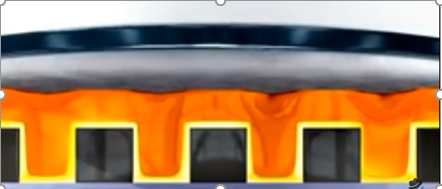
LAST STEP:

- The last is the packaging of the chips. In preparation for this step thin silver applied on the wafer.

- We will link the chip to the frame, these are the finest saw-blades. The chips are cut the wafer.

- The flip-chip method is used to bind the chip to the frame, which is sealed with a cover
No comments:
Post a Comment